


FAQ: What can Printed Circuit Board (PCB) jumpers do?
February 29th 2016A circuit board jumper is basically a conductor that gets soldered between two points on the board to make a connection.
There are two general reasons for adding PCB jumpers. The first is to correct a defect or implement a change after the board has been defined or assembled. Jumpers for correcting these types of problems are considered wires and get installed during or after assembly. Their routing, termination, and bonding are documented either by engineering instructions and drawing notations, or by engineering change notices.
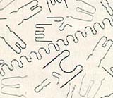
The second is when a PCB jumper is added during assembly but is considered a circuit component. It generally takes the form of a small copper wire or flat wire that is usually soldered using the same automated methods as for other board components.
In the old days, jumpers were often made up by hand. Today, there are jumpers designed to be placed on the circuit board by machine and automatically wave soldered and there are jumpers specifically designed for surface-mounting or for insertion in through-holes.
PCB jumpers can come in handy for a variety of scenarios. One example is where the installation of a few jumpers is an alternative to putting more traces or layers on the PCB itself. Here, it may be more economical to install jumpers rather than add a PCB layer comprised of just a few connections.
Another use of PCB jumpers is as a means of realizing "hard wire" programming of circuit board logic. For example, on a multifunction logic card, jumpers can be installed and then selectively cut as appropriate to permanently set the card options or configuration.
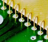
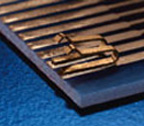
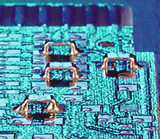
(There's a related device called a Surface Mount Jumper that resembles the PJ-Series. It also takes the form of a loop but it's designed specifically for SMT applications.)
There are two sizes of jumpers for surface mounting. Both are supplied on seven-inch reels. The SJ-Series is basically a piece of flat copper wire with a matte tin-over-nickel under plate finish. The device is formed so it loops up about 0.05 in. above the circuit board. Thus is has a low profile but also provides clearance above the board so it needn't be insulated. It can be either 0.08 or 0.12-in. long and 0.05 or 0.062-in. wide respectively.