


FAQ: What are printed circuit board (PCB) test points?
February 29th 2016What is a printed circuit board (PCB) test point?
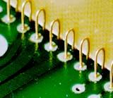
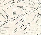
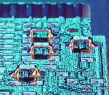
A surface-mount test point is basically a small wire loop designed as an attachment point for test probes on a circuit board containing surface-mount components. It is relatively small, about the same size as a standard chip capacitor package.
What is a surface-mount test point?
Surface-mount test points have become necessary as circuit board designs transitioned away from leaded devices toward surface-mounted versions. On a board that contains only surface-mount components, there may be no easy way to hook a test probe on for making measurements. That's because test probes are often fitted with either a spring-loaded J-hook that lets the operator clip to a component on the circuit board, or with sharp pointed ends designed to touch a trace or some other conductor on the board.
Of course, J-hooks were originally created in the days when circuit components had leads that stuck through the circuit board. It is relatively easy to clip a J-hook onto a lead to make a measurement. That changed when the electronics industry went to surface-mount components and most leads went away.
What materials are used in a surface-mount test point?
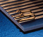
Surface-mount test points are typically formed from a phosphor bronze alloy. They have an ultra-low profile compatible with the component height dimensions of surface mount devices. Though they generally use copper conductors, they can also be obtained with silver-plate coatings. This version is an economical replacement for other kinds of test point products and is offered with a 0.0001-in. min. silver over 0.00005-in. min. copper plate.
How do you manufacture a surface-mount test point?
Some surface-mount test points are fabricated using a special forming process to accommodate mechanical stress on the bond that arises in a surface-mount design. This is accomplished by forming the flat wire design in a spiral wrap on the mounting base resulting in adhesion to the solder pad which requires in excess of 18 lb. of force to dislodge the test point from its solder pad. The profile accepts most commercially available spring clips and probes while providing a positive and secure anchor to the SMT board.
What formats are available for surface-mount test points?
Surface mount test points are available in two formats: bulk packaged and tape-and-reel configuration. The taped version is fully compatible with ANSI/EIA-481 standards. The recommended mounting pad dimensions are 0.185×0.135 in.
What are the advantages and disadvantages of surface-mount test points?
The advantages of surface-mount test points become clear in comparison to alternative methods of connecting test probes. As an alternative to surface-mount test points, the board fabricator can install posts or turrets at strategic points on the board for access by a test probe. The disadvantage is that posts can stick up a quarter-inch high or more. The height may be problematic if the enclosure is just super thin. The alternative is to touch the probe to a circuit trace on the board to take a measurement. But board traces are often coated with a material that protects against moisture. Making a connection involves poking through that coating. In this case, there is a possibility of compromising the protective coating.